


INFORMATION NEEDED IN CELLPHONE REPAIR
(objective: student must know how to take down notes for their repairs )
1. HISTORY (WHAT HAPPEN TO THE PHONE/HARDWARE/SOFTWARE)
2. SERIAL NO. (IMEI *#06#)
3. VERSION NO. (*#0000#)
4. BATTERY NO.
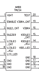
5. BOARD NO.
6. CPU NO.
7. MISSING PARTS
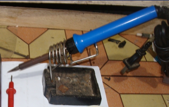
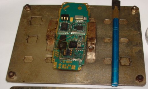
8. PRESENCE OF FLUX
MINOR REPAIRS
(objective: to be able to identify the types of repairs and phone problems)
1. NO AUDIO RECEPTION
2. NO AUDIO TRANSMISSION
3. NO RING TONE
4. DISPLAY MALFUNCTION
5. KEYPAD MALFUNCTION
6. INSERT SIM CARD
MAJOR REPAIRS
1. HANGING/AUTO SHUT OFF
2. WATER DAMAGED
3. CONTACT SERVICE
4. NOT CHARGING
5. NO POWER
6. NO SIGNAL
MINOR REPAIRS
1. NO AUDIO RECEPTION
DIAGNOSIS REMEDY
a.) SPEAKER/EARPIECE a.) TEST/LIFT PINS/REPLACE
b.) SPEAKER INTERFACE b.) CLEAN W/ERASER
c.) SMALL COMPONENTS c.) REHEAT/REPLACE
d.) LOST CONNECTION d.) RECONNECT/JUMPER
note: use schematic diagram to check the connection and
small components. from audio ic to speaker interface
e.) AUDIO IC (COBBA) e.) REHEAT/REBOLL/REPLACE
f.) BP (board problem) f.) RTO (return to owner)
note: before RTO try software trouble shooting first
2. NO AUDIO TRANSMISSION
DIAGNOSIS REMEDYa.) MIC/MOUTH PIECE a.) TEST /LIFT PINS/REPLACE
b.) MIC INTERFACE b.) CLEAN W/ERASER
c.) SMALL COMPONENTS c.) REHEAT/REPLACE
d.) LOST CONNECTION d.) RECONNECT/JUMPER
note: use schematic diagram to check the connection and
small components. from audio ic to mic interface
e.) AUDIO IC (COBBA) e.) REHEAT/REBOLL/REPLACE
f.) BP (board problem) f.) RTO (return to owner)
note: before RTO try software trouble shooting first
3. NO RING TONE
DIAGNOSIS REMEDYa.) BUZZER a.) TEST/LIFT PINS/REPLACE
b.) BUZZER INTERFACE b.) CLEAN W/ERASER
c.) SMALL COMPONENTS c.) REHEAT/REPLACE
d.) LOST CONNECTION d.) RECONNECT/JUMPER
note: use schematic diagram to check the connection and
small components. from UI ic to buzzer interface
e.) AUDIO IC (COBBA) e.) REHEAT/REBOLL/REPLACE
f.) BP (board problem) f.) RTO (return to owner)
note: before RTO try software trouble shooting first
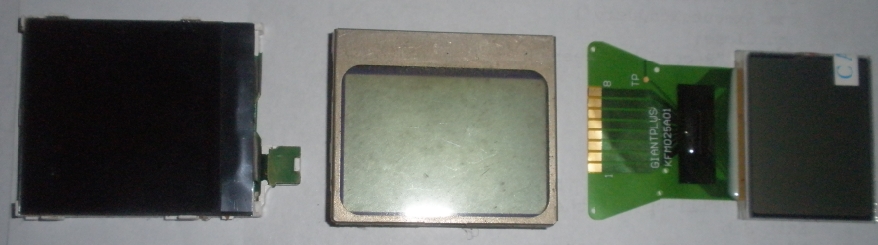
4. DISPLAY MALFUNCTION
DIAGNOSIS REMEDY
a.) LCD a.) REPLACE IF DAMAGED b.) LCD INTERFACE b.) CLEAN/VOLTAGE TEST /JUMPER
d.) LOST CONNECTION d.) RECONNECT/JUMPERc.) SMALL COMPONENTS c.) REHEAT/REPLACE
note: use schematic diagram to check the connection and
small components. from POWER IC to LCD interface
f.) BP (board problem) f.) RTO (return to owner)
note: before RTO try software trouble shooting first
5. KEYPAD MALFUNCTION
DIAGNOSIS REMEDY a.) CASING a.) FIT PROPERLY /REPLACE
b.) KEYPAD INTERFACE b.) CLEAN W/ERASER
c.) SMALL COMPONENTS c.) REHEAT/REPLACE
d.) LOST CONNECTION d.) RECONNECT/JUMPER
note: use schematic diagram to check the connection and
small components. from CPU to KEYPADTRANSISTOR
JUMPER TO GROUPMATES
e.) UPP/CPU (IF NECESSARY) e.) REHEAT/REBALL/REPLACE
f.) BP (board problem) f.) RTO (return to owner)
note: before RTO try software trouble shooting first
6. INSERT SIM CARD
DIAGNOSIS REMEDY a.) SIMCARD a.) TEST /REPLACE IF DAMAGED
b.) LCD INTERFACE b.) CLEAN/VOLTAGE TEST /JUMPER
c.) SMALL COMPONENTS c.) REHEAT/REPLACE
d.) LOST CONNECTION d.) RECONNECT/JUMPER
note: use schematic diagram to check the connection and
small components. from POWER IC to SIMCARD interface
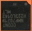
e.) POWER IC (CCONT) e.) REHEAT/REBOLL/REPLACE
f.) BP (board problem) f.) RTO (return to owner)
note: before RTO try software trouble shooting first
MAJOR REPAIRS
1. HANGING/AUTO SHUT OFF
DIAGNOSIS REMEDY
a.) BATTERY a.) TEST /SHOCK/ REPLACE
b.) BATTERY TERMINAL b.) LIFT PINS/RESOLDER/REPLACE
c.) BATTERY INTERFACE c.) CHECK IF SHORTED
d.) SMALL COMPONENTS d.) REHEAT/REPLACE
e.) LOST CONNECTION e.) RECONNECT/JUMPER
note: use schematic diagram to check the connection
and small components. from BATTERY interface and power lines
check legend of diagrams for power supply flow
f.) POWER IC (CCONT) f.) REHEAT/REBOLL/REPLACE
RF PROCESSOR (HAGAR) AUDIO IC (COBBA)
FLASH IC/MEMORY IC
RAM IC
g.) CRYSTAL OSCILLATOR g.) REHEAT/ REPLACE
REALTIME CLOCK
h.) BP (board problem) h.) RTO (return to owner)
note: before RTO try software trouble shooting first
2. WATER DAMAGED
1. DIS ASSEMBLE THE UNIT
2. SOAK WITH LACQUER THINNER BRUSH SLIGHTLY
3. AIR DRY USING HOT AIR SET AIR: 8 HEATER: 2 OR 3
4. ASSEMBLE THE UNIT
5. TEST.
IF PHONE STILL NO POWER FOLLOW THE PROCEDURE OF NO POWER
3. CONTACT SERVICE (CS)
USE UFS(TWISTER FLASHER) TO DETECT THE ERROR OF CONTACT SERVICE
IF
COBBA SERIAL IS 000000 TRY TO UPDATE THE PHONE FIRST DOUBLE CLICK
SET FAID IF STILL CS TRY TO FLASH THE PHONE INPUT MCU AND PPM. IF PHONE
STILL CS TRY TO REHEAT/REPLACE COBBA. IF STILL NO LUCK CPU IS THE
PROBLEM.
IF SERIAL NUMBER OR IMEI IS OOOOOOOO OO POSSIBLE
PROBLEM IS FLASH IC/MEMORY IC /RAM TRY TO FLASH IF STILL NO LUCK
REPLACE FLASH IC. IF STILL NO LUCK CPU IS THE PROBLEM.
4. NOT CHARGING
DIAGNOSIS REMEDY
a.) CHARGER a.) TEST / REPLACE
b.) BATTERY b.) TEST/ SHOCK/ REPLACE
c.) BATTERY TERMINAL c.) LIFT PINS/ RESOLDER/ REPLACE
d.) BATTERY INTERFACE d.) CHECK IF SHORTED
e.) CHARGING PINS e.) LIFT PINS/ RESOLED/ REPLACE
f.) CHARGING INTERFACE f.) CLEAN W/ ERASER
g.) SMALL COMPONENTS g.) REHEAT/REPLACE
h.) LOST CONNECTION h.) RECONNECT/JUMPER
note: use schematic diagram to check the connection and
small components. check positive BATTERY terminal interface
and power lines, power ic to charging ic and charging interface.
check legend of diagrams for power supply flow.
i.) CHARGING IC i.) REHEAT/REBALL/REPLACE
POWER IC (CCONT) j.) BP (board problem) j.) RTO (return to owner)
note: before RTO try software trouble shooting first
5. NO POWER
DIAGNOSIS REMEDY
a.) BATTERY a.) TEST /SHOCK/ REPLACE
b.) BATTERY TERMINAL b.) LIFT PINS/ RESOLDER/REPLACE
c.) BATTERY INTERFACE c.) CHECK IF SHORTED
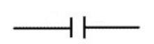
d.) SWITCH (S401) d.) TEST/REPLACE
e.) SMALL COMPONENTS e.) REHEAT/REPLACE
f.) LOST CONNECTION f.) RECONNECT/JUMPER
note: use schematic diagram to check the connection and
small components. from BATTERY interface and power lines
check legend of diagrams for power supply flow
g.) POWER IC (CCONT)(N201) g.) REHEAT/REBALL/REPLACE
RF PROCESSOR (HAGAR) AUDIO IC (COBBA)
FLASH IC/MEMORY IC
RAM IC
h.) CRYSTAL OSCILLATOR h.) REHEAT/ REPLACE
REALTIME CLOCK
i.) BP (board problem) i.) RTO (return to owner)
note: before RTO try software trouble shooting first
6. NO SIGNAL
DIAGNOSIS REMEDY
a.) SIMCARD a.) REPLACE IF DAMAGED/ TEST
b.) ANTENNA b.)REPLACE IF DAMAGED
c.) ANTENNA SWITCH c.) REHEAT/TEST BY JUMPER/REPLACE
d.) FILTERS /COUPLERS d.) REHEAT/REPLACE
e.) SMALL COMPONENTS e.) REHEAT/REPLACE
f.) LOST CONNECTION f.) RECONNECT/JUMPER
note: use schematic diagram to check the connection and
small components. Check legend for signal flows rx and tx flows.
g.) RF PROCESSOR (HAGAR) g.) REHEAT/REBALL/REPLACE
AUDIO IC (COBBA ) POWER IC (CCONT)(N201)
FLASH IC/MEMORY IC
RAM IC
REALTIME CLOCK
h.) CRYSTAL OSCILLATOR h.) REHEAT/ REPLACE
i.) BP (board problem) i .) RTO (return to owner)
note: before RTO try software trouble shooting first
TX (TESTING OF TRANSMISSION)
PRESS : # AND CALL ...... REQUESTING
GOOD: RESULT UNKNOWN /REQUEST NOT COMPLETED
DEFFECTIVE: NOT DONE/ NO NETWORK COVERAGE
RX (TESTING OF RECEPCION)
PRESS: MENU + SETTINGS + PHONE SETINGS + NETWORK SELECTION + MANUAL ..... SEARCHING
GOOD: 2 TO 3 NETWORKS
DEFFECTIVE: 1 NETWORK /NO NETWORK FOUND
TIPS: FLUCTUATING SIGNALS REHEAT REPLACE FILTERS/COUPLERS
SIGNAL DROPS AFTER 10 SECONDS: AUDIO IC/PA REHEAT OR REPLACE